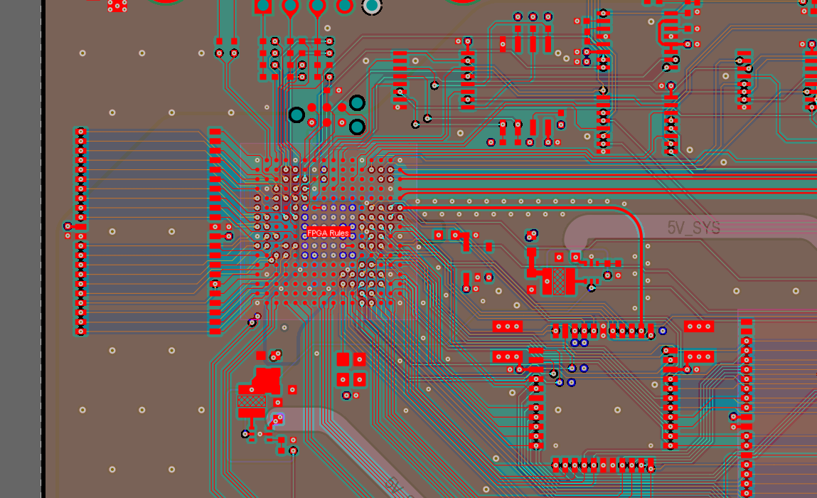
After a week of work on the schematic and layout and another week reviewing both by me, and a friend that is learning electronics, it is time for production of PCB.
This is a 6 layer board with;
- 100µm line / spacing.
- 450µm via pads with 200µm drill hole. The bias are filled and capped, so I can place them in pad. That is mostly needed in the BGA package of the FPGA.
- The board is around 450mm long and 65mm wide.
So let's see how this works when it comes back from PCB manufacturing as well as I have soldered all the components in place.